Inertial NEMS for Nanosensor Applications Based on Inorganic Nanotubes
Patents for licensing
Inertial sensors for motion detection are being incorporated into an increasing number of portable devices, including diverse IoT applications, mobile phones, wearable electronics, automotive systems and medical diagnostic sensors. The current size reduction trend in electronics, requires incorporation of reliable nanoelectromechanical systems (NEMS) into nanosensors, yet market applications of NEMS are currently limited by high costs of fabrication and inconsistent quality. A new technology developed by a group of researchers from the Weizmann Institute, provides a unique, highly reproducible structure for inertial nanosensors, with high durability at the nanoscale and with a detection mechanism based on the piezoresistive effect. The invention further extends application opportunities of extremely small portable electronics, which, with the increasing use of spatial awareness in reduced size electronics and IoT, is expected to witness increasing market demand.

The Need
Current microelectromechanical system (MEMS) fabrication technologies for inertial sensors are limited by the ability to produce sufficiently small sensors, which are required for numerous applications. Lack of measurement repeatability in varied environments is a limiting factor in current systems, and measurement drift over time prevents the extended use of current smallest devices, prohibiting use, for instance, in critical applications (e.g., military systems). The wide-spread size reduction trend, pushing MEMS into the NEMS scale, is also prominent in consumer electronics, where an increasing number of components in mobile phones and wearable electronics are being compacted to fit within limited space and power constraints. A similar trend has been seen in the medical field, where medical implants for diagnosis and patient monitoring are constantly being reduced in order to enable extremely high accuracy and to minimize invasiveness. Similarly, automotive systems, such as airbag control and rollover detection, require many smaller and lighter inertial sensors, and demand is only increasing as vehicles incorporate more smart technologies.
The growing pressure to reduce the size of electronics is driving innovation in large-scale production of more miniaturized components. The presented new inertial nanosensor technology provides a unique opportunity to develop reliable and durable inertial sensors that are in the nanoscale, increasing functionalities in portable electronic devices.
The Solution
A novel structure for inertial sensors with a motion detection mechanism based on the piezoresistive effect that enables drastic size reduction of the sensing device to the nanoscale. The novel device incorporates inorganic nanotubes for increased sensitivity and reliability.
Technology Essence
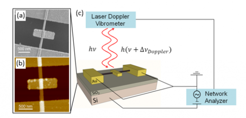
The structure of the inertial sensor consists of a suspended nanotube clamped between metallic pads at its ends, with a suspended pedal attached at the top (see Figure 1). The pedal is off-centered with respect to the nanotube, so each end of the pedal stands at a different distance from the nanotube. The structure was fabricated using electron-beam lithography, followed by wet-etching and critical point drying. In order to measure the oscillatory behavior of the torsional resonators, a DC bias voltage and a smaller AC drive voltage are applied between the substrate and the pedal. The alternating voltage between the substrate and the pedal combined with the offset of the center of the pedal with respect to the nanotube, creates an oscillatory net torque on the pedal, leading to periodic twisting the nanotube. The pedal vibration detection can be detected using an electric signal.
(a) Scanning electron microscope image and (b) atomic force microscope image of the nanotube-based inertial sensor. (c) The inertial sensor is actuated by applying voltage between the substrate and the offset pedal, which is attached to the nanotube.
Advantages and Advantages
Applications
Nanosensors can be used for various applications including:
IoT devices
Medical implants and devices.
Development Status
Successful operation of the inertial nanosensor device was demonstrated (published in: Nano Lett. 2017, 17;1: 28-35 [1]). Yeda Research and Development, the technology transfer arm of the Weizmann Institute of Science, has filed a patent application and is working with Prof. Joselevich’s lab to develop a proof-of-concept prototype with an electrical output rather than the optical signal described in the publication.
Market Opportunity
Market demand will be driven by incorporation of inertial sensors into a wide range of mass-produced consumer electronics, medical sensors and vehicles. As wearable electronics become widespread, the demand for inertial sensor technology is expected to be the most prominent in consumer devices markets. The global sensor market is projected to reach $241 billion by 2022, with an 11.3% CAGR, with the NEMS sector estimated to have a growth rate of 14.3%.
As NEMS technology develops in industry, it is expected to integrate with existing MEMS, to reduce production costs and increase product accuracy. The inertial sensors MEMS market, including oscillators, gyroscopes, accelerometers and inertial combos, is currently estimated at $4.4 billion and is expected to grow ever faster than previously, due to widespread adoption of sensors to enable wireless and internet connectivity, with a CAGR between 15-20%. NEMS will also increase the value of several IoT hardware markets. The IoT market as a whole is projected to reach $46 billion by 2024 with a CAGR of 17%.
Yeda ("Knowledge" in Hebrew) Research and Development Company Ltd. is the commercial arm of the Weizmann Institute of Science (WIS) and is the second company of its kind established in the world.
WIS is one of the world’s leading multidisciplinary basic research institutions in the natural and exact sciences. It is located in Rehovot, Israel, just south of Tel Aviv. It was initially established as the Daniel Sieff Institute in 1934, by Israel and Rebecca Sieff of London in memory of their son Daniel. In 1949, it was renamed for Dr. Chaim Weizmann, the first President of the State of Israel and Founder of the Institute.
Yeda initiates and promotes the transfer to the global marketplace of research findings and innovative technologies developed by WIS scientists. Yeda holds an exclusive agreement with WIS to market and commercialize its intellectual property and generate income to support further research and education.
Since 1959 Yeda has generated the highest income per researcher compared to any other TTO worldwide. Weizmann has generated a number of groundbreaking therapies, such as Copaxone, Rebif, Tookad, Erbitux, Vectibix, Protrazza, Humira, and recently the CAR-T cancer therapy Yescarta.
Yeda performs the following activities:
◣ Identifies and assesses research projects with commercial potential.
◣ Protects the intellectual property of WIS and its scientists.
◣ Licenses WIS' inventions and technologies to industry.
◣ Establishes new Startup companies based in WIS Intellectual Property
◣ Channels funding from industry to research projects.
Our portfolio covers a broad spectrum of the natural sciences, including:
◣ Agriculture and Plant Genetics, including Bio-fuels
◣ Chemistry and Nanotechnology
◣ Environmental Sciences and Solar Energy
◣ Mathematics and Computer Science
◣ Medical Devices
◣ Pharmaceuticals and Diagnostics
◣ Physics and Electro-Optics
◣ Research Tools
Create your free account to connect with Yeda and thousands of other innovative organizations and professionals worldwide
Send a request for information
to Yeda
Technology Offers on Innoget are directly posted
and managed by its members as well as evaluation of requests for information. Innoget is the trusted open innovation and science network aimed at directly connect industry needs with professionals online.
Need help requesting additional information or have questions regarding this Technology Offer?
Contact Innoget support