Optical Bus for a Multi-Core Processor
Patents for licensing
The exponential increase in computational power over the last decades is running into a bottle-neck – the only way of getting more computing power per chip is to integrate multiple-cores, but the problem with multiple-cores is the complex wiring system, used for inter-core communication. This technology, developed at the Weizmann Institute of Science propose a radically new idea that replaces wires and fibers altogether, by an appropriately designed integrated optical chip layer that serves the same purpose with less complexity. It eliminates the use of wires thus saving valuable space, reducing power consumption and subsequently internal heat production. It further allows for high number of interconnected processors on the same chip and improves inter-core connectivity by 100-1000-fold, ultimately increasing computational power.

The Need
With the global race for more compact electronics, chipmakers are constantly seeking for innovative ways to reduce power consumption, component volumes, and heat production. In parallel, technology developments have increased end-user demands for faster and more efficient systems, requiring either increased clock-speed or multicore processors and subsequent complex inter-core communication. Both alternatives suffer from major drawbacks as increased clock-speed results in higher power consumption and internal heat production, and efficient inter-core communication enabled by complex wire bus systems, takes space, consume energy, and produce excess heat.
The only existing alternative to wires is optical fibers, which while reducing the internal heat production are still limited by complex wiring networks and one-dimensional optical data transmission. The stagnant clock rate, growing chip complexity, and the limiting number of integrated core processors, demands a robust inter-core data transmission platform that will be more efficient, less complex, and enable better multicore connectivity.
The Solution
A single compact on-chip optical layer, compatible with CMOS fabrication technologies, that replaces the tangle of wires and fibers.
Technology Essence
This invention designed by transformation optics, involves a compact optical bus, comprised of a planar waveguide on silicon chips where light is confined in a layer by total internal reflection. The layer is made of silicon that has a high refractive index, sandwiched between layers of silica (glass) with a much lower index. The height of the highly refractive layer is carefully designed to provide a specific refractive index profile, dictated by the layer thickness. A light management system selectively activates specific illumination ports embedded within the waveguide; the emanating light is then focused onto reflectors, or Bragg mirrors, which lead to light ray emission at specific partner points. In a similar manner, the light can be simultaneously focused onto a plurality of photodetectors within the waveguide, each of which communicates with a separate processor core. Bus geometry can be adjusted to match computer processor or core layout requirements.
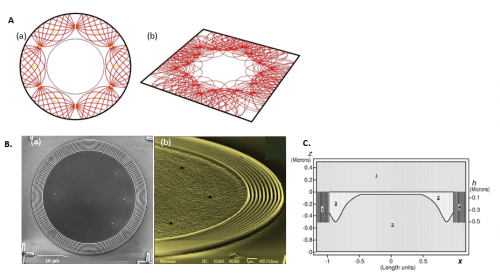
A) Schematic top view of light propagation in a propagation layer for different optical bus geometries. (a) Absolute focusing: any number of points are optically connected (demonstrated for six points). These points can be located at any position on the ring (b) Rectangular waveguide structure. Communication is possible between multiple points and on different waveguides geometries. B) Electron-microscope images of a prototype manufactured by e-beam lithography. (a) Top view and (b) Side view: Bragg mirror around the device. C) Schematic cross-sectional view of an optical bus. 1,3: Lower and upper non-propagation layers; 2: light propagation layer, 4: Bragg mirror. The effective refractive index, defined by the thickness profile of the propagating silicon layer, causes light propagation to follow specific propagation paths with unique and exclusive sets of focal points.
Applications and Advantages
Advantages
Increased computing power
Reduced heat output
Applications
The proposed innovation is applicable for a full range of markets integrating electronic technologies including:
Consumer electronics
Robotics
Signal processing
Telecommunication
Information processing
Development Status
Miniature prototypes have been fabricated (Published in: O. Bitton, R. Bruch, and U. Leonhardt, Phys. Rev. Applied 10, 044059 (2018) [1]). Future work will focus on developing models that match industry size and performance standards, to bring it closer to commercialization. A patent application was submitted for this invention.
Yeda ("Knowledge" in Hebrew) Research and Development Company Ltd. is the commercial arm of the Weizmann Institute of Science (WIS) and is the second company of its kind established in the world.
WIS is one of the world’s leading multidisciplinary basic research institutions in the natural and exact sciences. It is located in Rehovot, Israel, just south of Tel Aviv. It was initially established as the Daniel Sieff Institute in 1934, by Israel and Rebecca Sieff of London in memory of their son Daniel. In 1949, it was renamed for Dr. Chaim Weizmann, the first President of the State of Israel and Founder of the Institute.
Yeda initiates and promotes the transfer to the global marketplace of research findings and innovative technologies developed by WIS scientists. Yeda holds an exclusive agreement with WIS to market and commercialize its intellectual property and generate income to support further research and education.
Since 1959 Yeda has generated the highest income per researcher compared to any other TTO worldwide. Weizmann has generated a number of groundbreaking therapies, such as Copaxone, Rebif, Tookad, Erbitux, Vectibix, Protrazza, Humira, and recently the CAR-T cancer therapy Yescarta.
Yeda performs the following activities:
◣ Identifies and assesses research projects with commercial potential.
◣ Protects the intellectual property of WIS and its scientists.
◣ Licenses WIS' inventions and technologies to industry.
◣ Establishes new Startup companies based in WIS Intellectual Property
◣ Channels funding from industry to research projects.
Our portfolio covers a broad spectrum of the natural sciences, including:
◣ Agriculture and Plant Genetics, including Bio-fuels
◣ Chemistry and Nanotechnology
◣ Environmental Sciences and Solar Energy
◣ Mathematics and Computer Science
◣ Medical Devices
◣ Pharmaceuticals and Diagnostics
◣ Physics and Electro-Optics
◣ Research Tools
Create your free account to connect with Yeda and thousands of other innovative organizations and professionals worldwide
Send a request for information
to Yeda
Technology Offers on Innoget are directly posted
and managed by its members as well as evaluation of requests for information. Innoget is the trusted open innovation and science network aimed at directly connect industry needs with professionals online.
Need help requesting additional information or have questions regarding this Technology Offer?
Contact Innoget support