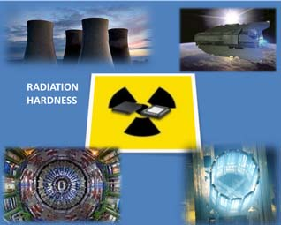
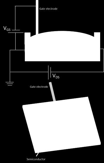
CSIC through the Instituto de Microelectrónica de Barcelona - Centro Nacional de Microelectrónica, has developed a novel JFET (Junction Field-Effect Transistor) which is very suitable to be used in high-radiation-level environments such as Space, high-flying aircraft, particles accelerator or radio-medical equipment. Due to its particular configuration, the device presents very high radiation hardness.
Industrial partners from the electronic industry focused on radiation detection are being sought to collaborate through a patent license agreement.
JFET switch operating in harsh radiation environments
JFET devices are widely used as switches or as a passive protection element. However, none of them is ideal for high radiation applications because their fabrication request the use of an inter-level oxide, which fails under expositions to high radiations level. Furthermore the use of n-doped substrates in electronics devices improving their electrical properties, unlikely increases their vulnerability to the radiation, making them not suitable to operate in high radiation environments.
Thus, one of the relevant research lines of modern power electronics is the search for appropriate devices for power distribution circuits and systems control that are capable of operating in high radiation environments. The novel JFET device due to its particular ring junction's configuration presents a very high radiation hardness which is very suitable to be used in high-radiation environments such as space, aeronautics, as well as nuclear power plants or radiomedical equipment.
Main innovations and advantages
Its main application is in Space and nuclear reactors in power plants, however, can be also used in high-flying aircraft, particles accelerator, or any electronic equipment or component that suffers high radiation like radiomedical equipment.
Advantages:
· Device robust to ionizing and non-ionizing damage.
· Better device design which allows a better injection of carriers into the channels.
· Higher active area (40%) · Very good current capability (x6 former detectors) compared to formers devices.
· Uniform voltage distribution over the device and very control of channel depletion.
· Very high drift region which increases (x3 former detectors) the breakdown voltage of the device preventing early breakdown.
