CSIC and the University of Oporto have developed a method that combines lithographic printing
techniques, aluminium anodizing for the manufacture of highly ordered nanoporous alumina templates
and metal sputtering by which metal nanostructures with the same ordering pattern are obtained.
These nanostructures can be used in different magnetic and nanoelectronic devices.
Industrial partners from the nanotechnology are being sought to collaborate through a patent licence
agreement.
An offer for Patent Licensing
Nanoporous templates with different geometry for
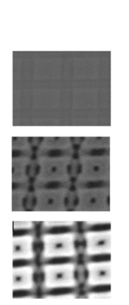
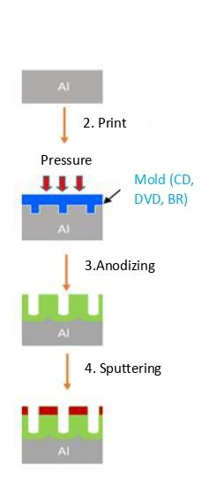
nanostructured metal coatings Figure 1: Outline the processes for obtaining ordered nanostructures (on the left) and the corresponding images after processes 2,3 and 4, for the case of cubic symmetry (on the right) The method consists of the following steps (Figure 1):
1. Starts from high purity aluminium laminates.
2. The mould (Cd, DVD and BR discs) is pressed onto the laminate, printing the predefined pattern os the particular disc on it. This process can be performed multiple times, changing the print angle to obtain templates of different geometry (cubic, triangular, rhombus symmetry).
3. By means of an electrochemical anodizing process the aluminium is oxidized and by self-assembly originates a template with ordered nanopores respecting the pattern previously printed.
4. By sputtering on the surface is obtained a metal coating that respects the aforementioned pattern.
In particular, it allows the production of metal nanostructures of different ferromagnetic materials of high applicability.
Main innovations and advantages
· The moulds used are low cost and large surface area. The printingprocess is short (2 hours) and easily mechanizable.
· A single anodizing process is performed, increasing corrosionresistance and providing better adhesión than bare metal.
· The market for aluminium nanostructured materials templates iscontinuously growing thanks to its high profitability.
· The possibility of manufacturing ferromagnetic nanostructured coatingsoffers new alternatives in the field of magnetic materials for magneticsensors and new recording media.
· New possibilities of application of these ordered nanostructures fornanophotonic devices (microlasers, portable sensors) and magnionic(transmit information faster and with lower energy expenditure).
