Nanoscale Electronic Spin Polarizer and Enhanced Magnetoresistance for Memory
Patents for licensing
Spintronics has a large impact on daily life, being the backbone of computing and electronic applications. The reduction in the size of spintronic elements is of central importance for efficient information processing. At the atomic scale, electronic transport is very sensitive to the fine details of the electronic orbital structure. Using this sensitivity, we provide methodologies that control and explore atomic-scale charge, transmit up to fully spinpolarized current by systematic orbital modifications and, in addition, amplify magneto-resistive effects of nanoscale magnetic elements while retaining a large signal, without the need for rare metals or complicated device structure.

The Need
While conventional electronics is based on the charge of electrons, exploiting the additional spin degree of freedom
offers advantages for electronics and computing applications. The most central requirement from a spin-based
device is the ability to generate highly spin-polarized currents of a single spin type. Highly spin-polarized currents at
the nanoscale are extremely important for modern electronics and quantum control. However, devices that can filter
electronic currents with significant spin polarization become increasingly challenging and are yet to be realized in
the nanoscale. An additional challenge in modern electronics is to minimize the size of memory bits while
maintaining a large signal for accurate reading of the stored information. Current memory storage devices that used
read heads based on the anisotropic magneto-resistance (AMR) effect, following by the giant magneto-resistance
(GMR) and tunneling magneto-resistance (TMR) effects have reached a maximum 20% change in resistance for
junctions made of relatively simple ferromagnetic materials. Further increase in the sensitivity of such memory
elements requires the use of sophisticated production techniques, the use of expansive materials, the use of multilayered architectures, and, in some cases, the use of complicated electronics to amplify the low signal. An
interesting approach that does not require a complicated architecture and can overcome these limitations is to
scale down to nano-size in order to provide a large magneto-resistance effect.
The Solution
Prof. Oren Tal and his group developed novel methods that generate spin polarization currents at nanoscale enabling spintronic miniaturization, spin filtering, and enhanced magnetoresistance.
Technology Essence
When current passes through an atomic-sized constriction, quantum confinement dictates that electronic transport is governed by the fine details of the local electronic structure. Suitable atomistic conditions can also affect the balance between spin-up and spin-down currents. Prof. Tal and his team took advantage of this sensitivity to efficiently manipulate spin-dependent transport by modifying the structure and composition of an atomic-scale conductor. They found that the formation of a nickel oxide (NiO) atomic junction between two nickel electrodes leads to highly efficient spin filtering that allows only one spin-type to flow through the constriction. This is explained in view of the orbital hybridization between low-coordinated Ni and O atoms, resulting in the emergence of local halfmetallicity.
In addition, there is a special bonding properties of conjugated oligoacene molecules to ferromagnetic surfaces which the team used for enhanced AMR effect. The adsorption process involves hybridization between the delocalized orbitals of the molecule and the highly-spin polarized d orbitals of the metal electrodes. This hybridization results in preferential conductance through the spin polarized orbitals, leading to at least one order of magnitude enhancement in magnetoresistance.
Applications
Advantages
Development Status
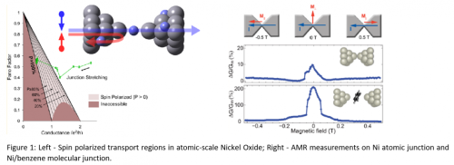
Prof. Tal and his team showed that nickel-oxide (NiO) atomic junctions made by oxidation of an atomic bridge between two nickel wires exhibit up to 100% spin-polarized conductance. The extremely high spin polarization was found to exist without the need of applying external magnetic fields. The team found that the degree of spin polarization can be tuned effectively by mechanical strain to yield a remarkable atomic-scale conductor with one dominant spin-polarized conduction channel. The team demonstrated, additionally, that spin filtering can be significantly enhanced by local chemical modifications at the single-atom level and that a minor change in the local atomic structure (i.e. the incorporation of oxygen between the Ni electrodes) can dramatically alter spin-transport properties.
Furthermore, Prof. Tal and his team demonstrated that adding a single-molecule junctions based on nickel electrodes and benzene molecules can yield a significant anisotropic magnetoresistance (AMR) of up to ∼200%2. It was shown that magnetoresistance can be mechanically tuned by changing the distance between the electrodes and that there is an optimal molecular orientation with respect to the ferromagnetic metal electrodes for maximum AMR due to efficient spin-selective orbital hybridization. This emphasizes the important role of geometrical considerations in determining the spin transport properties of metalâ molecule interfaces.
Market Opportunity
Yeda ("Knowledge" in Hebrew) Research and Development Company Ltd. is the commercial arm of the Weizmann Institute of Science (WIS) and is the second company of its kind established in the world.
WIS is one of the world’s leading multidisciplinary basic research institutions in the natural and exact sciences. It is located in Rehovot, Israel, just south of Tel Aviv. It was initially established as the Daniel Sieff Institute in 1934, by Israel and Rebecca Sieff of London in memory of their son Daniel. In 1949, it was renamed for Dr. Chaim Weizmann, the first President of the State of Israel and Founder of the Institute.
Yeda initiates and promotes the transfer to the global marketplace of research findings and innovative technologies developed by WIS scientists. Yeda holds an exclusive agreement with WIS to market and commercialize its intellectual property and generate income to support further research and education.
Since 1959 Yeda has generated the highest income per researcher compared to any other TTO worldwide. Weizmann has generated a number of groundbreaking therapies, such as Copaxone, Rebif, Tookad, Erbitux, Vectibix, Protrazza, Humira, and recently the CAR-T cancer therapy Yescarta.
Yeda performs the following activities:
◣ Identifies and assesses research projects with commercial potential.
◣ Protects the intellectual property of WIS and its scientists.
◣ Licenses WIS' inventions and technologies to industry.
◣ Establishes new Startup companies based in WIS Intellectual Property
◣ Channels funding from industry to research projects.
Our portfolio covers a broad spectrum of the natural sciences, including:
◣ Agriculture and Plant Genetics, including Bio-fuels
◣ Chemistry and Nanotechnology
◣ Environmental Sciences and Solar Energy
◣ Mathematics and Computer Science
◣ Medical Devices
◣ Pharmaceuticals and Diagnostics
◣ Physics and Electro-Optics
◣ Research Tools
Create your free account to connect with Yeda and thousands of other innovative organizations and professionals worldwide
Send a request for information
to Yeda
Technology Offers on Innoget are directly posted
and managed by its members as well as evaluation of requests for information. Innoget is the trusted open innovation and science network aimed at directly connect industry needs with professionals online.
Need help requesting additional information or have questions regarding this Technology Offer?
Contact Innoget support