Showing 1 to 15 of 2391 results
![Floatable Photovoltaic System to generate Electric Energy. Advantage of cooling the Photovoltaic System generating more power unde[…]](https://static3.innoget.com/images/bgpremium.png)

Floatable Photovoltaic System to generate Electric Energy. Advantage of cooling the Photovoltaic System generating more power unde[…]
Patents for licensing BPE e.K.
Application and method of producing cyclic compounds in olefin metathesis reaction
Innovative Products and Technologies Technology Transfer Office (University of Warsaw)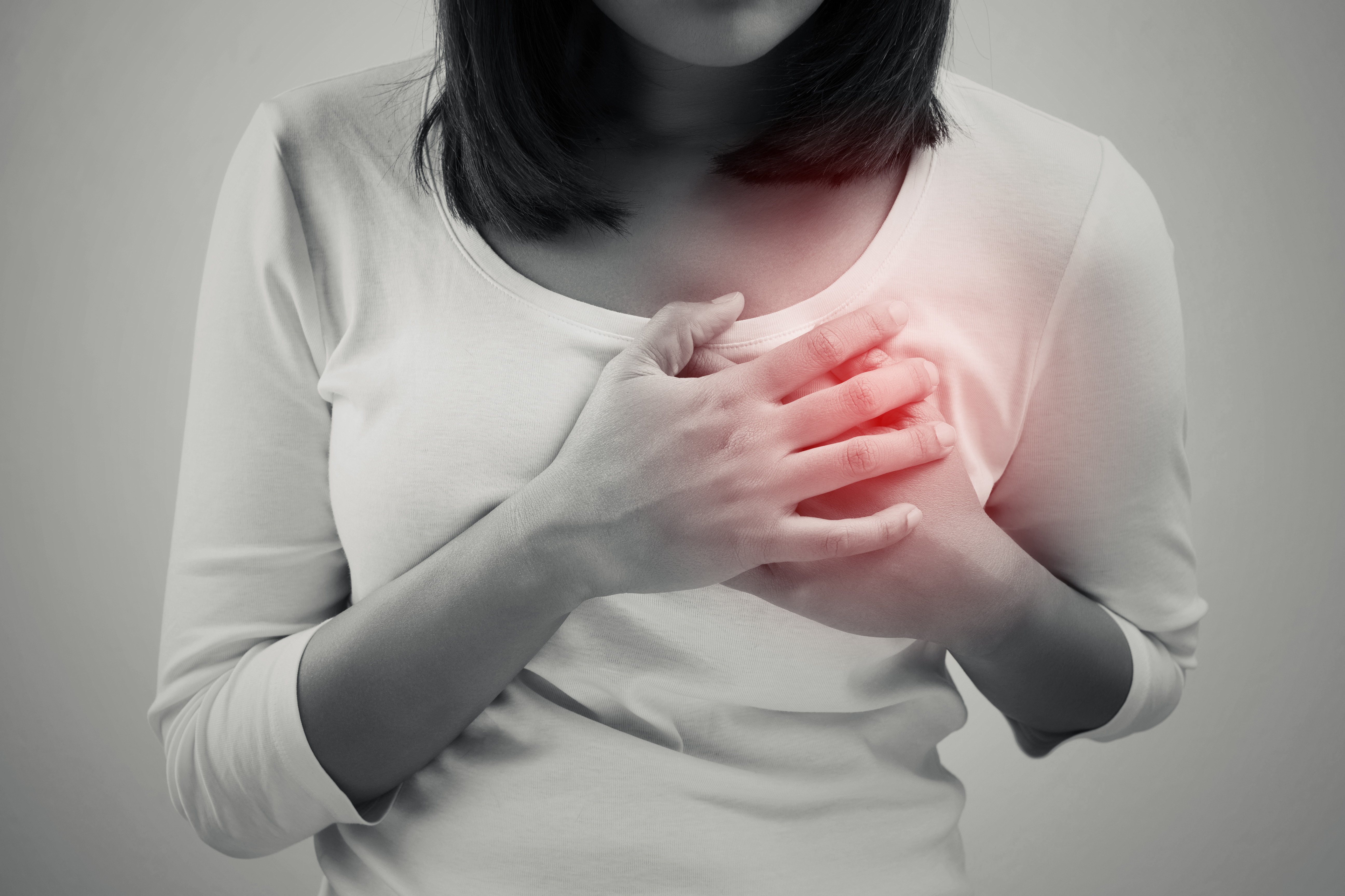

Circular RNA biomarkers for heart failure diagnostics
Patents for licensing Luxembourg Institute of Health
Tools for gender sensitisation in educational institutions
Patents for licensing Universidad de Alicante![Alteration of hierarchy-dependant transcription in multigene complexes by perturbing dominant members using site-specific nuclease[…]](https://static8.innoget.com/uploads//1219ff576edbf33629fa050b21dced5990c918c4.png)

Alteration of hierarchy-dependant transcription in multigene complexes by perturbing dominant members using site-specific nuclease[…]
Innovative Products and Technologies CSIR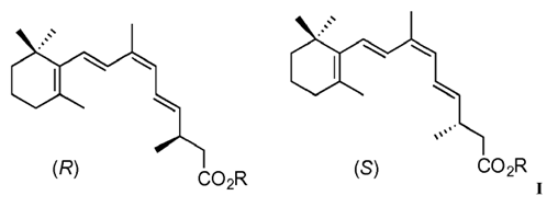

Stereoselective synthesis of 9-CIS.13,14- Dihydroretinoic acid and its ethyl esters
Patents for licensing CINBIO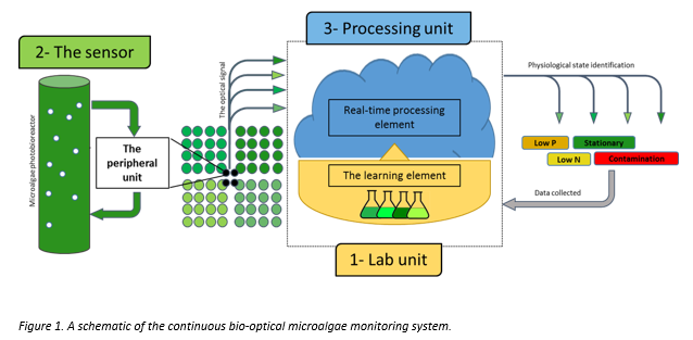

Continuous Biooptical Monitoring of Microalgae Crops
Patents for licensing Yeda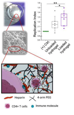
Mimetic lymph nodes for immune cell culture
Patents for licensing ICMAB-CSIC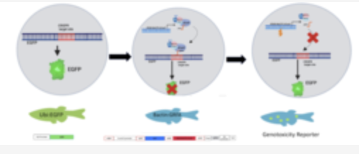

Real-time zebrafish reporter assay for monitoring tissue-specific genotoxicity
Innovative Products and Technologies Georgetown University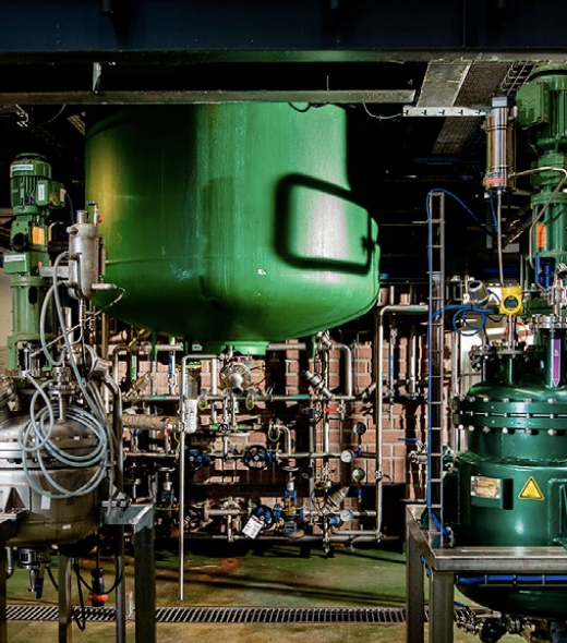

Piloting, scale-up and manufacturing equipment and expertise
Research Services and Capabilities Bio Base Europe Pilot Plant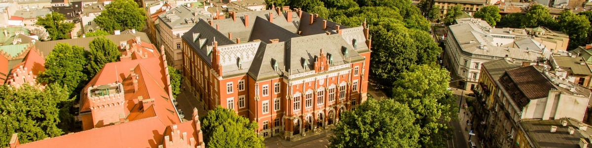

Protein disulphide isomerase inhibitors
Patents for licensing Jagiellonian University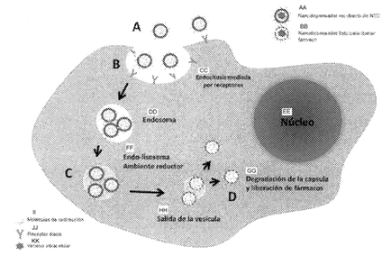
Coverage of carbon nanotubes for use as an anchoring system for nano and micrometer devices with therapeutic activity
Patents for licensing CINBIO

Technique to obtain a medical image from elastic properties of tissues
Patents for licensing CSIC - Consejo Superior de Investigaciones Científicas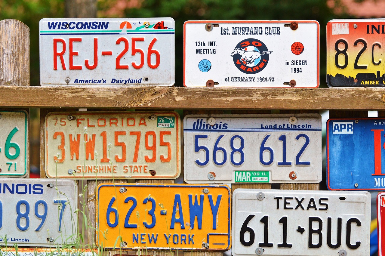
Mobile device for real-time license plate recognition without Internet connection
Patents for licensing Universidad de Alicante